Flashgal (set 1, Kyugo logo): Difference between revisions
From Citylan
Jump to navigationJump to search
mNo edit summary |
mNo edit summary |
||
| (4 intermediate revisions by the same user not shown) | |||
| Line 13: | Line 13: | ||
|+ style="background:silver" | PCB Infos | |+ style="background:silver" | PCB Infos | ||
|- | |- | ||
|name || ''' | |name || '''[http://adb.arcadeitalia.net/?mame=flashgalk flashgalk on Arcade Database]''' | ||
|- | |- | ||
|description || '''Flashgal (set 1, Kyugo logo)''' | |description || '''Flashgal (set 1, Kyugo logo)''' | ||
| Line 59: | Line 59: | ||
|6x || [[27128|M5L27128K]] || bottom PCB 6a,7a,8a,9a,10a,11a || dumped | |6x || [[27128|M5L27128K]] || bottom PCB 6a,7a,8a,9a,10a,11a || dumped | ||
|- | |- | ||
|2x || [[PROM| | |2x || [[PROM|TBP24S10N]] || top PCB 1f,1h || dumped | ||
|- | |||
|1x || [[PROM|TBP24S10N]] || top PCB 1j || dumped, see notes | |||
|- | |- | ||
|2x || [[PROM|TBP18S030]] || top PCB 2c,5j || dumped | |2x || [[PROM|TBP18S030]] || top PCB 2c,5j || dumped | ||
| Line 88: | Line 90: | ||
!status | !status | ||
|- | |- | ||
|1x || [[18v8|PAL12L6]] || top PCB 4m || | |1x || [[18v8|PAL12L6]] || top PCB 4m || dumped | ||
|- | |- | ||
|1x || [[12l6|PAL12L6]] || top PCB 5n || | |1x || [[12l6|PAL12L6]] || top PCB 5n || dumped | ||
|- | |- | ||
|1x || [[16v8|GAL16V8B]] || bottom PCB 1j || | |1x || [[16v8|GAL16V8B]] || bottom PCB 1j ||see notes | ||
|} | |} | ||
| Line 103: | Line 105: | ||
==Notes== | ==Notes== | ||
top PCB is marked: "MADE IN JAPAN" on component side<br> | top PCB is marked: "MADE IN JAPAN" on component side<br> | ||
bottom PCB is marked: "CVG-48C" and "1984" on component side | bottom PCB is marked: "CVG-48C" and "1984" on component side<br> | ||
the PROM @1j was broken (detail pic 1), Corrado made a substitution for it with a GAL (detail pic 2). The project files are available at [http://www.jammarcade.net www.jammarcade.net] | |||
----- | ----- | ||
update 20180410: pics and better description | update 20180410: pics and better description | ||
| Line 109: | Line 112: | ||
==Files== | ==Files== | ||
<gallery widths="150px"> | <gallery widths="150px"> | ||
Image:1504_top_PCB_component_side.jpg|top PCB component side | |||
Image:1504_top_PCB_component_side_marks.jpg|top PCB component side marks | |||
Image:1504_bottom_PCB_component_side.jpg|bottom PCB component side | Image:1504_bottom_PCB_component_side.jpg|bottom PCB component side | ||
Image:1504_bottom_PCB_component_side_marks.jpg|bottom PCB component side marks | Image:1504_bottom_PCB_component_side_marks.jpg|bottom PCB component side marks | ||
Image: | Image:1504_bottom_PCB_component_side_detail1.jpg|bottom PCB component side detail 1 | ||
Image: | Image:1504_bottom_PCB_component_side_detail2.jpg|bottom PCB component side detail 2 | ||
</gallery> | </gallery> | ||
Latest revision as of 15:17, 20 October 2024
| dumper | Corrado Tomaselli |
| date | 10/03/2017 |
| emulator | MAME 0.184 |
| dev | Osso |
| name | flashgalk on Arcade Database |
| description | Flashgal (set 1, Kyugo logo) |
| year | 1985 |
| manufacturer | Kyugo / Sega |
Technical references
CPUs
| QTY | Type | clock | position | function |
|---|---|---|---|---|
| 1x | Z8400AP5-Z80ACPU | top PCB 3e | 8-bit Microprocessor - main | |
| 1x | LH0080A-Z80ACPU | top PCB 5k | 8-bit Microprocessor - main | |
| 2x | AY-3-8910 | top PCB 6d,6e | Programmable Sound Generator - sound | |
| 1x | audio amplifier | top PCB 3a | Audio Amplifier - sound | |
| 1x | oscillator | 18.432 | bottom PCB 6t |
ROMs
| QTY | Type | position | status |
|---|---|---|---|
| 8x | M5L2764K | top PCB 2f,2h,2j,2k,4f,4h,4j,4k | dumped |
| 1x | HN482732AG | bottom PCB 4a | dumped |
| 3x | 2764 | bottom PCB 9h,10h,11h | dumped |
| 6x | M5L27128K | bottom PCB 6a,7a,8a,9a,10a,11a | dumped |
| 2x | TBP24S10N | top PCB 1f,1h | dumped |
| 1x | TBP24S10N | top PCB 1j | dumped, see notes |
| 2x | TBP18S030 | top PCB 2c,5j | dumped |
RAMs
| QTY | Type | position |
|---|---|---|
| 1x | SRM2016C-10 | top PCB 2m |
| 3x | SRM2016C-10 | bottom PCB 3m,10m,11m |
| 4x | HM6148P-8 | bottom PCB 3j,3k,5k,5l |
| 3x | SRM2114C3 | bottom PCB 4r,7l,7m |
PLDs
| QTY | Type | position | status |
|---|---|---|---|
| 1x | PAL12L6 | top PCB 4m | dumped |
| 1x | PAL12L6 | top PCB 5n | dumped |
| 1x | GAL16V8B | bottom PCB 1j | see notes |
Others
1x 18x2 edge connector (top PCB)
1x 50 pins flat cable connector from top PCB to bottom PCB
1x trimmer (volume)(top PCB VR1)
2x 8 DIP switches banks (top PCB DPSW1,DPSW2)
Notes
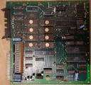
top PCB is marked: "MADE IN JAPAN" on component side
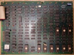
bottom PCB is marked: "CVG-48C" and "1984" on component side
the PROM @1j was broken (detail pic 1), Corrado made a substitution for it with a GAL (detail pic 2). The project files are available at www.jammarcade.net
update 20180410: pics and better description
Files
-
top PCB component side
-
top PCB component side marks
-
bottom PCB component side
-
bottom PCB component side marks
-
bottom PCB component side detail 1
-
bottom PCB component side detail 2
1504


