Flash Point (Japan, bootleg set 1): Difference between revisions
(Created page with "{| style="float: right;" border="1" cellpadding="3" cellspacing="0" |+ style="background:silver" | EMU Infos |- |dumper || f205v |- |date || 10/11/2019 |- |emulator || MAME 0....") |
mNo edit summary |
||
| Line 13: | Line 13: | ||
|+ style="background:silver" | PCB Infos | |+ style="background:silver" | PCB Infos | ||
|- | |- | ||
|name || ''' | |name || '''[http://adb.arcadeitalia.net/?mame=fpointbj fpointbj on Arcade Database]''' | ||
|- | |- | ||
|description || '''Flash Point (Japan, bootleg set 1)''' | |description || '''Flash Point (Japan, bootleg set 1)''' | ||
Latest revision as of 15:54, 20 October 2024
| dumper | f205v |
| date | 10/11/2019 |
| emulator | MAME 0.69 |
| dev |
| name | fpointbj on Arcade Database |
| description | Flash Point (Japan, bootleg set 1) |
| year | 1989 |
| manufacturer |
Technical references
CPUs
| QTY | Type | clock | position | function |
|---|---|---|---|---|
| 1x | SCN68000CAN64 | MHz(9.998@15) | main PCB u7 | 16/32-bit Microprocessor - main |
| 1x | Z0840006PSC | MHz(5.996@6) | main PCB u52 | 8-bit Microprocessor - sound |
| 1x | YM2151 | MHz(1.998@23) -MHz(3.997@24) | sound PCB | FM Operator Type-M (OPM) - sound |
| 1x | YM3012 | MHz(1.998@2) | sound PCB | D/A Converter (DAC) - sound |
| 1x | TL084CN | - | sound PCB | Operational Amplifier - sound |
| 1x | TDA2003 | - | main PCB u75 | Audio Amplifier - sound |
| 1x | oscillator | 20.000 | main PCB xl1 | |
| 1x | oscillator | 24.000 | main PCB xl2 |
ROMs
| QTY | Type | position | status |
|---|---|---|---|
| 1x | M27256 | main PCB 1 | dumped |
| 2x | TMS27PC512 | main PCB 2,3 | dumped |
| 5x | TMS27PC512 | ROMs PCB 4,5,6,7,8 | dumped |
| 1x | N82S123N | ROMs PCB 17a | dumped |
| 1x | 63S141N | ROMs PCB 1b | dumped |
RAMs
| QTY | Type | position |
|---|---|---|
| 1x | MK6116N-15 | main PCB u55 |
| 2x | MCM2018AN45 | main PCB u36,u37 |
| 2x | HY6264LP-10 | main PCB u1,u4 |
| 8x | MCM2018AN45 | ROMs PCB 5a,6a,13a,5b,6b,13b,5f,6f |
| 2x | KM62256ALP-10 | ROMs PCB 1f,4f |
PLDs
| QTY | Type | position | status |
|---|---|---|---|
| 1x | GAL16V8-25HB1 | ROMs PCB 18a | read protected |
| 1x | PLHS18P8AN | main PCB u51 | read protected |
| 1x | unknown PAL (DIP24-300mil) | main PCB u13 | read protected |
Others
1x 28x2 JAMMA edge connector
2x 50 pins flat cable connector from main PCB to ROMs PCB
1x DIP40-600mil connector from main PCB to sound PCB
1x trimmer (volume)(main PCB V1)
2x 8 DIP switches banks (main PCB u58,u60)
Notes
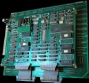
main PCB is marked: "F/P" on component side
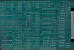
main PCB is marked: "F/P" on solder side
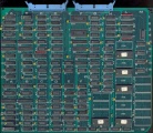
ROMs PCB is marked: "F/P" on component side
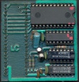
sound PCB is marked: "LC" on component side ("LC" is the Italian for "Lato Componenti" which translates to "Components Side")
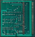
sound PCB is marked: "LS" on solder side ("LS" is the Italian for "Lato Saldature" which translates to "Solders Side")
Files
-
assembled PCBs
-
main PCB component side
-
main PCB solder side
-
ROMs PCB component side
-
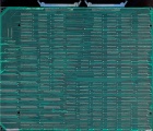
ROMs PCB solder side
-
sound PCB component side
-
sound PCB solder side
-
Disclaimer
-
Start
-
Select
-
In game 1
-
In game 2
1679
